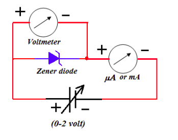
To draw the V-I characteristic of Zener diode and to determine Zener breakdown voltage.
Zener diode is a heavily doped PN junction diode. Due to heavily doped, its
depletion layer is very thin and is order of micrometer. The forward bias characteristic of Zener
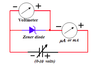
diode is same as the normal PN junction diode but in reverse bias it has different characteristic.
Initially, a negligible constant current flow through the zener diode in its reverse bias but at
certain voltage, the current becomes abruptly large. This voltage is called as zener voltage. This
sudden and sharp increase in zener current is called as zener breakdown.
The zener diode with breakdown voltage Vz is revverse biased and is connected in parallel with the load resistance RL across which a constant output voltage is desired.
For an input voltage Vi greater than the zener diode's voltage Vz, the zener diode will maintain a constant output voltage Vo= Vz across the load resistance RL.
When the input voltage is increased slowly, a very small current flows through the zener diode. It offers a very high resistance to the current and the whole of input appears across the output terminals. Consequently in this range, the output terminals. Consequently in this range, the output voltage increases linearly with the input voltage. Once the input voltage is greater than Vz, zener diode offers a very small resistance to the current. Consequently a large current flows in the circuit and the voltage drop across the series resistance Rs will increase maintaining the voltage drop across RL at constant Vo= Vz.
Animation of the experiment:--
Click here to perform the simulation
| S.No. | VF (volts) | IF (mA) |
|---|---|---|
| 1 | ||
| 2 | ||
| 3 | ||
| 4 |
| S.No. | VR (volts) | IR (uA) |
|---|---|---|
| 1 | ||
| 2 | ||
| 3 | ||
| 4 |
The V-I characteristic of Zener diode indicates that characteristic of Zener diode in forward bias is same as PN junction diode. In reverse bias, a negligible constant current flow through the zener diode but the current becomes abruptly large at certain voltage. This voltage is called as zener voltage. This sudden and sharp increase in zener current is called as zener breakdown. Vknee=0.7 volt and VZ= 9 volt.